|
Wide
Band Gap Semiconductors Group at YSU
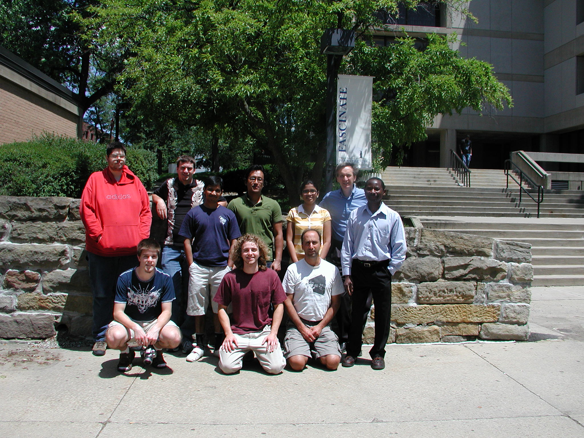
Dr. Oder and and graduate student Krishna Kundeti, Spring 2017 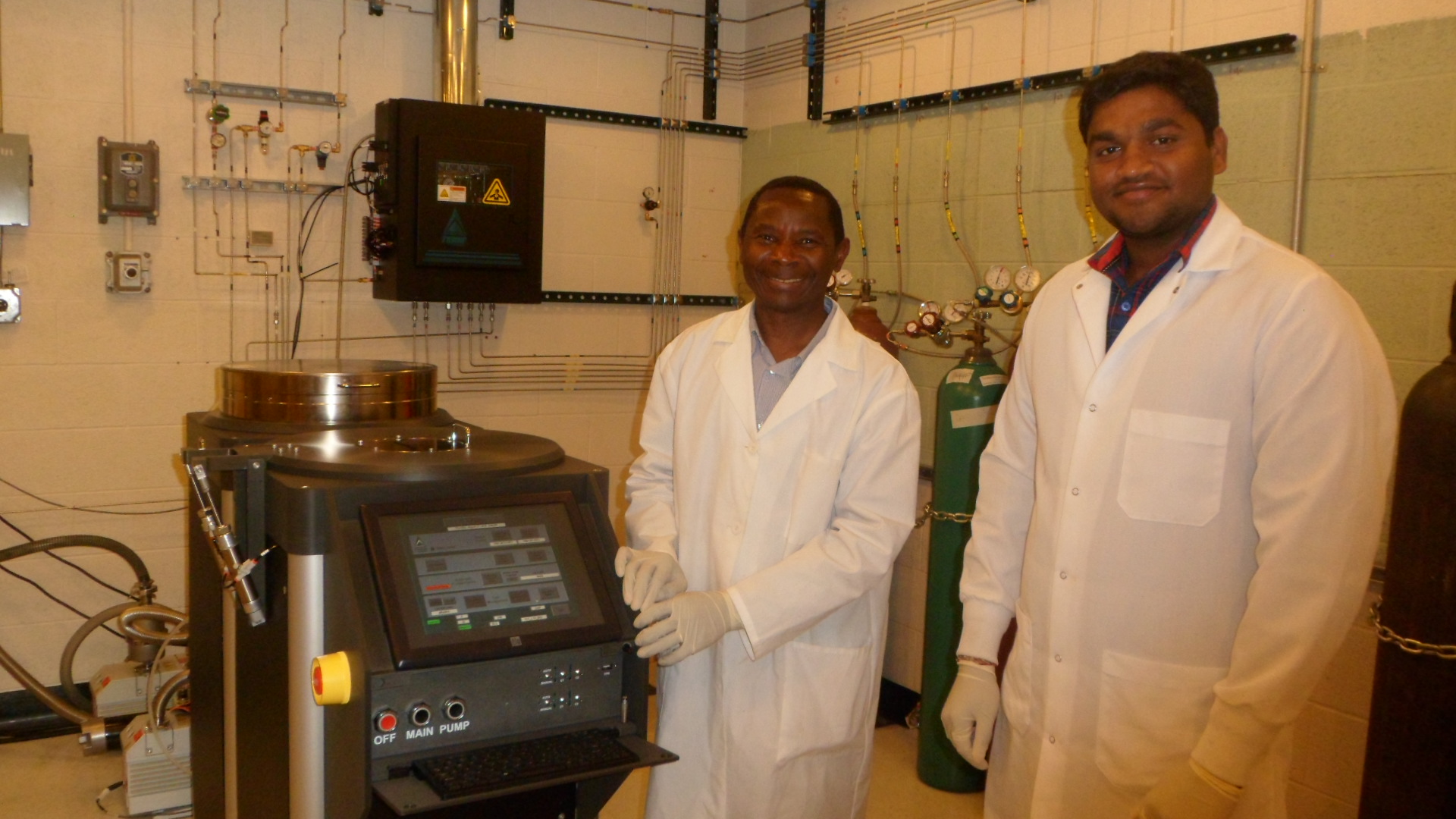 Dr. Oder and some of his student research assistants, Spring 2013  L-R: Andrew Smith, Nawayandra
Shakya, Michael McMaster, Dr. Oder, Scott Alfredo, Clayton Reakes and
Mark Freeman
Why Wide Band Gap Semiconductors?A Wide Band Gap (WBG) semiconductor in general terms can be defined as a semiconductor with an energy band gap (EG) above 2 eV. Included in this group are the group III-nitrides, silicon carbide (SiC), zinc selenide (ZnSe) etc. The focus of our group is on the group III-nitrides, silicon carbide and zinc oxide. Present-day commercial satellites, modern jet aircrafts, automobile engines, sub-sea well logging systems, etc require thermal radiators to dissipate heat generated by the functional electronics. High temperature electronic systems for such functions require electronic devices that retain their functions and reliabilities up to the desired operation temperature as well as an interconnection technology on a substrate to form an electronic circuit with long-term operation capability. Currently, these electronics are based on traditional semiconductors such as silicon or gallium arsenide, which would fail if they were not properly cooled. The cooling system introduces serious drawbacks including addition of a substantial amount of weight, which lowers the efficiency and reliability of the devices. As a result, wide band gap semiconductors such as group III-nitrides, silicon carbide and zinc oxide have recently attracted a great deal of attention. These semiconductors offer the possibility of realizing exciting new electronic devices for high power, high temperature and high frequency operations enabling substantial savings, increased performance and reliability. The III-nitrides and zinc oxide in particular can be used in a variety of opto-electronic devices operating in shorter wavelength regions than could be possible with silicon or gallium arsenide. Group III-nitrides: The group III-nitrides comprise gallium nitride (GaN, EG = 3.4 eV), aluminum nitride (AlN, EG = 6.2 eV) indium nitride (AlN, EG = 0.8 eV) an their alloys. Silicon carbide:
Silicon carbide (SiC) exists as a family of crystals known as polytypes. The difference among the polytypes is in the arrangement of layers of silicon (Si) and carbon (C) and over 200 polytypes of SiC are known to exist. Only one cubic (zincblende) polytype 3C, with EG = 2.39 eV exists and the rest are hexagonal (wurtzite). Of the wurtzite polytype, the important ones are 4H (with EG = 3.27 eV) and 6H (with EG = 3.02 eV). Silicon carbide possesses extremely high thermal, chemical, and mechanical stability. Its extreme mechanical stability is the reason for its use as a coating for drill bits and saw blades. Because of its large band gap energy, the thermal generation of electron-hole pairs in SiC is many orders of magintude lower at any given temperature compared to silicon. This makes it possible to build "dynamic" memories (DRAMs) in SiC that only need to be refreshed about once every 100 years at room temperature! This also makes it possible to operate SiC devices at temperatures as high as 650 °C without degradation in electrical performance. The breakdown electric field in SiC is about 8 times higher than in silicon, making SiC very attractive for fabricating high-voltage power switching transistors. Collaboration with our group:
At
present, we have collaboration with the GaN group at
Kansas State University and with
the Condensed
Matter group at Auburn
University. We warmly welcome collaboration with other groups
working
in this field and we encourage you to contact Dr. Tom N. Oder
(tnoder@ysu.edu).
|
- Research
Facilities
-

Kurl Suss MJB# Mask Aligner

Trion Minilock ICP/RIE Plasma Etching System
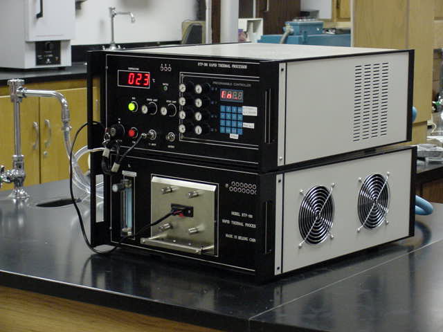
Rapid Thermal ProcessorHe-Cd Laser for Photoluminescence Measurements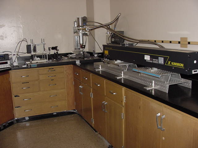
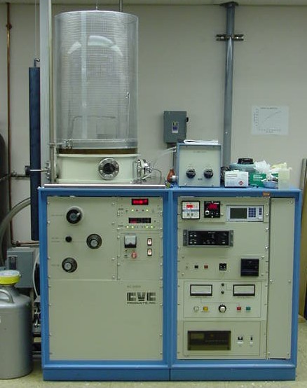
Sputter Deposition System

Mask Aligner
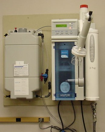
De-Ionized Water System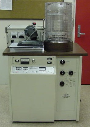
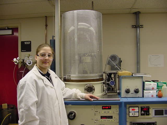
Vacuum Annealing System

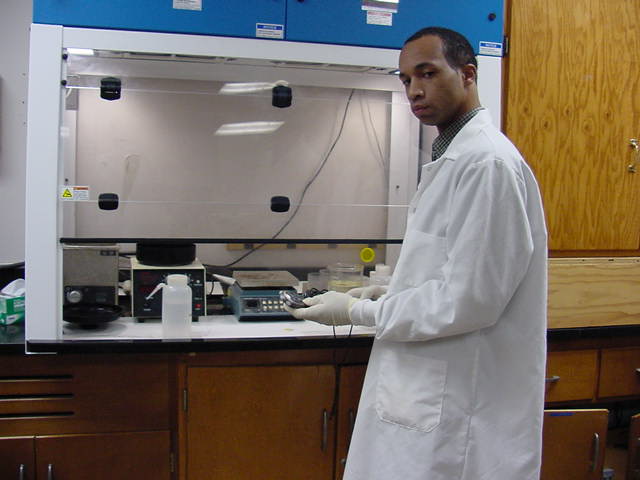
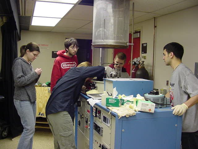
Electrical Characterization Station
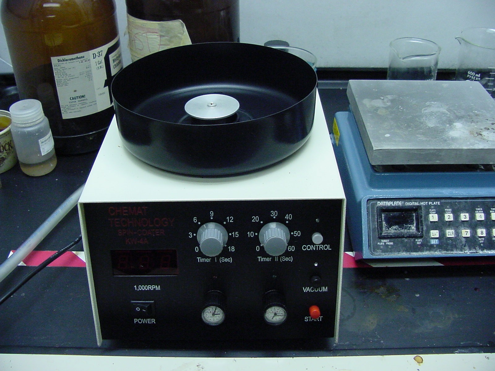
Resist Spin Coater
Dr. Jim Andrews and Dr. Oder at the Atomic Force Microscope (AFM) from Agilent, model 5500.
APS Meeting 2009

Dr. Oder explains his research at the APS 2009 meeting
 Ashley Snipes (High School Intern, Summer
2011)
|
 Andrew Smith at the MRS Meeting in Boston,
MA
|
||
 Michael McMaster (BS student, Physics)
|
 Nagaraju Velpukonda (MS student,
Electrical Engineering)
|
||
 Devin
at the new Karl-Suss Mask Aligner
|
 Keyona Woods (Intern From East High
School,
Summer 2010)
|
||
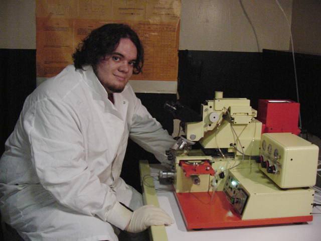
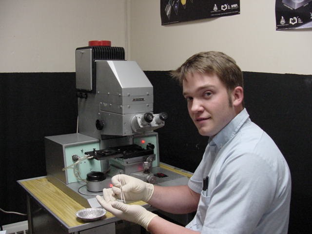
 Michael Nycz at the PL
System
|
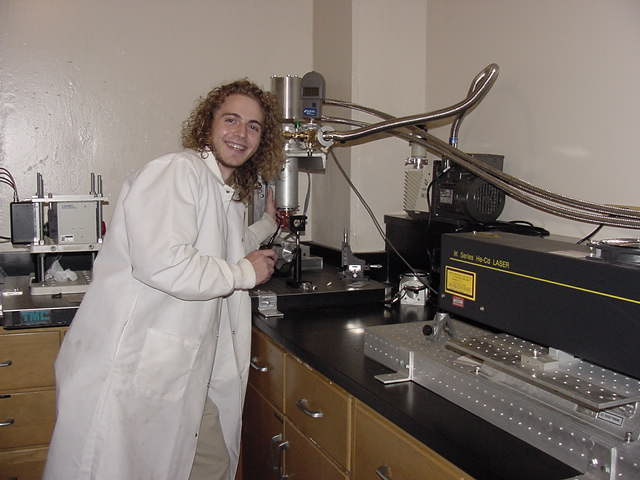
 Luch
at QUEST
|
|
|
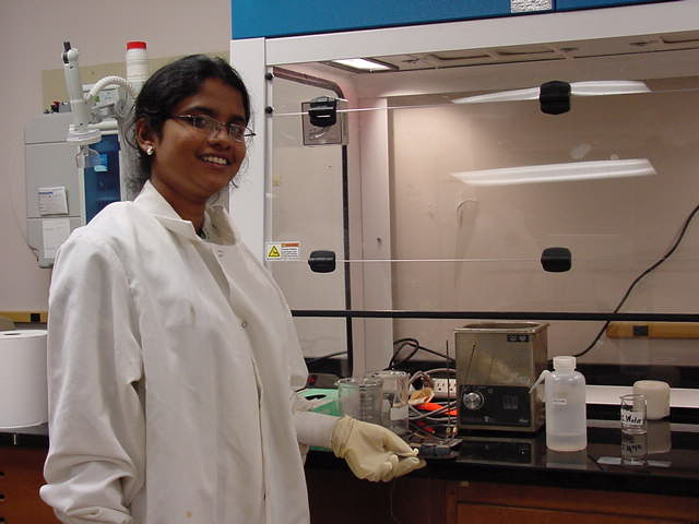
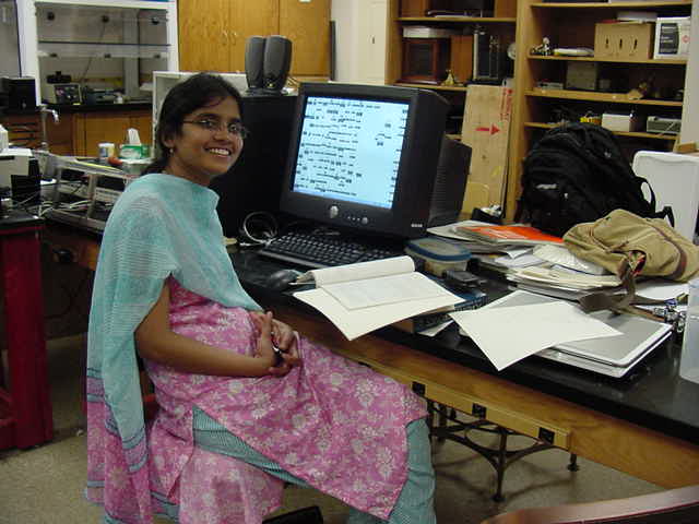 Rani Kummari performing
data
analysis
|
 James Aldridge preparing a
sample
|
||
 Bijayandra Shakya (BJ)
|
 James and BJ doing
I-V-T measurements
|
|
|
 Dr.
Oder with High School
students
|
 Dr. Ta-Lun Sung
(Visiting Prof. from Taiwan)
|
||
 Condensed Matter Physics Class 5830
|
 |
||
 Mark Barlow preparing a sample
|
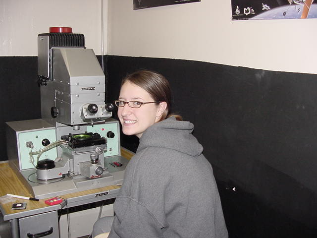
 Edward Sutphin at the mask aligner
|
||
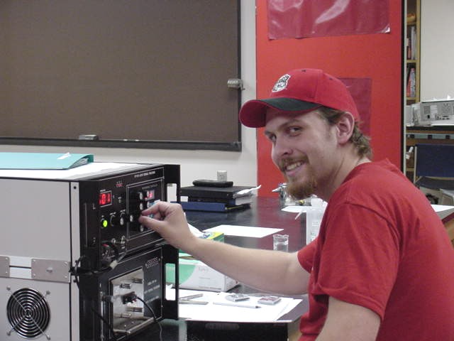 Aaron Schott doing RTP annealing
|
 Sara Schaefer at the mask aligner
|
||
 Rani
Kummari preparing samples
|
 Photonic, Optical,
Electronic Materials
(POEM) Group
|
||
 Mark Del Fraino at work
|
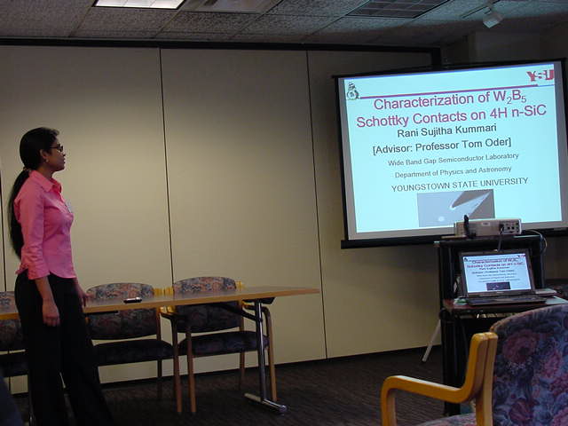 Rani Presents
|
||
 Snowflake Kicovic at the sputtering system
|
 Pam Martin Using I-V
Characterization System
|
|
|
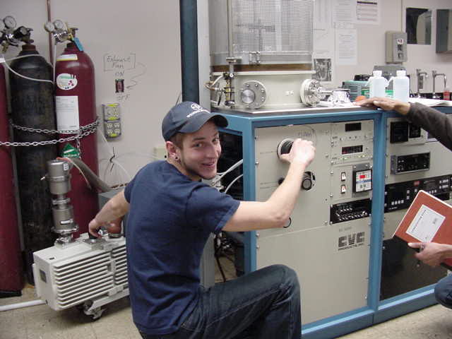
 Matt
Crummel installing the Sputtering System
|
 Loren Webb
|
||